Zhengzhou Abrasive Materials and Tools Cutting-edge Research Institute, Wang Guangzu, Central China Diamond Tool Manufacturing Co., Ltd., Wang Yun, Henan Iger Abrasive Materials Co., Ltd., Qin Yu / Article
Diamond is a material with excellent physical, chemical, and mechanical properties. Over the past few decades, diamond's extremely high hardness and excellent wear resistance have been well-utilized in materials, abrasives, automotive components, and other forms in the fields of machinery, petroleum, cutting tools, aerospace, and semiconductor processing, playing a substitutive role. In fact, diamond also exhibits outstanding properties in areas such as electronics, optics, thermodynamics, and acoustics, but these achievements have not yet been effectively developed.

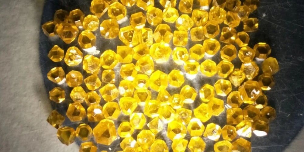
- The Diamond Battery That Can Generate Power for Thousands of Years
The prototype of the diamond nuclear battery can be traced back to the research of British physicist Henry Moseley in 1913, who demonstrated an experiment showing radiation-induced current generation. In the 1950s and 1960s, the aerospace industry considered applying Moseley’s research to spacecraft to provide long-term power. At the same time, companies were also researching nuclear detection batteries and wireless receivers for other fields.
However, these nuclear batteries still had certain issues regarding safety and conductivity. In this regard, the emergence of synthetic diamonds offers a promising solution. Diamond is the hardest known material and can be arranged or supported by semiconductors through special equipment. The core power of the battery is replaced by the β decay from nuclear material.
β decay is the process by which a nuclear atom (composed of protons and neutrons) releases surplus particles in order to reach a stable ratio of protons to neutrons, while emitting many β particles (high-energy electrons or positrons). When these β particles excite semiconductor materials, they generate electric current, which is then converted into electrical energy. However, because β particles are emitted from various directions, only a small portion of them hit the semiconductor, reducing the amount of generated electricity and efficiency.
The diamond battery utilizes chemical vapor deposition (CVD) technology, which is widely used in synthetic diamond production. Researchers adjust the CVD process and add a diluent containing the isotope carbon-14 to generate diluted diamonds. The nuclear resonance fuel inside, under β radiation, can provide a long-lasting, rechargeable battery.
"Carbon-14 is chosen as the raw material because it emits short-range radiation, which is quickly absorbed by any solid material," explained Professor Neil Fox. The Bristol team stated that their diamond battery (containing 1 gram of carbon-14) generates low power, only a few microwatts, much lower than a typical AA battery (size 5). As a result, the current applications are limited to small, low-power devices like sensors and pacemakers, and it is not yet suitable for laptops or smartphones.
It is worth noting that the UK company Arkenlight is preparing to bring this diamond battery to the market. The company's first micro-battery product is expected to be released in the second half of 2023 (Tencent News).
- Diamond and Silicon Carbide Substrate Cooling Technology
This technology can efficiently cool high-power GaN High Electron Mobility Transistors (HEMTs), allowing power amplifiers to operate stably at high power levels. High-frequency GaN-HEMT power amplifiers have been applied in long-range radio fields such as radar and radio communications and are expected to be used in weather radar to observe local heavy rain or in the upcoming 5G millimeter-wave mobile communication protocol. For radar or radio communication systems that use microwave to millimeter-wave frequencies, increasing the output power of GaN-HEMT power amplifiers used for transmission will extend the propagation distance of radio waves, enabling radar to cover a larger observation range and achieving longer distances and higher capacity communication.
Although silicon carbide (SiC) substrates have relatively high thermal conductivity, for devices with increasingly higher output power, substrates with better thermal conductivity are needed to effectively transfer heat from the device to the cooling structure. Monocrystalline diamond, which has excellent thermal conductivity—almost five times that of SiC substrates—is considered an efficient heat dissipation material.
To bond monocrystalline diamond to devices as cooling materials, the normal production process typically uses an argon (Ar) beam to remove impurities. However, this process can form a low-density damaged layer on the surface and weaken the bond that the monocrystalline diamond may form. Additionally, when using insulating films like SiN for bonding, the thermal resistance of SiN can reduce the thermal conductivity.
To prevent the argon beam from forming a damaged layer on the diamond surface, Fujitsu developed a technology that protects the surface with an extremely thin metal film before exposure to the argon beam. To ensure a flat surface (for good bonding at room temperature), the thickness of the metal film needs to be limited to 10 nanometers or thinner. This technology has been proven to prevent the formation of a damaged layer on the diamond surface after exposure to the argon beam, thereby increasing the bonding strength and enabling monocrystalline diamond to bond with SiC substrates at room temperature.
As a result, this technology can be used to produce GaN-HEMT power amplifiers with higher output power. When applied in systems such as weather radar, GaN-HEMT power amplifiers used for transmitters are expected to increase the radar's observable range by 1.5 times, allowing for faster detection of cumulus clouds that could lead to sudden heavy rain, thus improving disaster prevention (Zhongzi Network).
- Nano-Diamond Thermal Paste, Doubling Thermal Conductivity
Thermal paste is crucial as the filler between a CPU and a heatsink. The thermal conductivity of common thermal pastes is around 10 W/m·K. Inex has launched a nano-diamond thermal paste with a thermal conductivity of up to 17 W/m·K, doubling the thermal performance. The model of this thermal paste is JP-DX2, which claims to use high-quality diamond thermal materials manufactured with nanotechnology, forming a fine molecular structure that provides excellent thermal conductivity.
What does this mean? Most common thermal pastes have a thermal conductivity of less than 10 W/m·K, with some high-quality ones reaching around 10-13 W/m·K. Of course, the best thermal conductivity is still achieved by liquid metal, which easily exceeds 70 W/m·K, with some exceeding 100 W/m·K, which is 5-10 times that of regular thermal pastes.
In addition to doubling its thermal conductivity, the JP-DX2 thermal paste also has excellent chemical stability, is non-corrosive, anti-oxidant, non-toxic, and not easily volatile. It can be stored for up to 3 years before use and can be used for up to 4 years once applied. Its operating temperature range is very broad, from -150°C to 350°C, with a recommended temperature range of -140°C to 340°C, which far exceeds the temperature range required for CPU cooling (Fast Technology).
- N-type Conductive Channel Diamond Field-Effect Transistor
The NIMS team in the United States has developed the world's first metal-oxide-semiconductor field-effect transistor (MOSFET) driven by a diamond n-type channel. This achievement is of great significance for the development of environmentally durable complementary metal-oxide-semiconductor (CMOS) integrated circuits, represented by standard electronic IC devices, which integrate multiple devices onto a single semiconductor substrate. It also marks an important step forward for diamond’s application in power electronics.
Diamond semiconductors have material properties such as an ultra-wide bandgap (5.45 eV), high breakdown field strength (10 MV/cm), high carrier saturation drift velocity, and high thermal conductivity (22 W/cm·K), along with excellent device quality factors. Using a diamond substrate allows for the development of high-temperature, high-frequency, high-power, and radiation-resistant electronic devices, overcoming technical bottlenecks such as self-heating effects and avalanche breakdown. In fields like 5G/6G communications, microwave/millimeter-wave integrated circuits, detection, and sensing, the development of diamond semiconductors plays a crucial role, especially in extreme environments like high temperatures and high radiation (e.g., near reactor cores), where they offer outstanding performance and reliability. As a result, diamond semiconductors are recognized as the most promising new semiconductor material and are hailed as the "ultimate semiconductor material."
In recent years, with the advancement of diamond growth technology, power electronics, spintronics, and microelectromechanical system (MEMS) sensors that can operate under high temperatures and strong radiation conditions, there has been an increasing demand for the monolithic integration of peripheral circuits based on diamond CMOS devices. To take full advantage of diamond’s excellent properties and achieve the integration of control systems with outstanding environmental stability, high-power CMOS technology is highly anticipated. Manufacturing CMOS integrated circuits requires both p-type and n-type channel MOSFETs.
Currently, diamond semiconductor technology is relatively mature, but n-type doping of diamond remains a global challenge. Over the years, numerous studies have explored theoretical calculations and experimental methods to find suitable elements and doping techniques for achieving low-resistance n-type diamond doping, but have not yielded satisfactory results. A major reason for this is that previous research has mainly been based on silicon single-crystal doping theories. The main impurity elements used include boron, phosphorus, sulfur, and lithium, which are incorporated into single-crystal diamond or microcrystalline diamond films during the growth process or through ion implantation methods. However, the conductivity of the doped films is low, and the electron mobility is poor, making them unsuitable for use in electronic devices. For example, nitrogen is a deep-level impurity in diamond, with a room-temperature activation energy of 1.7 eV, making it difficult to provide sufficient carriers at room temperature. Phosphorus has a slightly shallower energy level, but its conductivity at room temperature is also weak. When phosphorus enters diamond, it readily forms phosphorus-vacancy pairs, making it difficult for its electrons to be released. To date, no suitable donor impurity has been found. From this perspective, the development of a new doping theory is an urgent task (DT Semiconductor).
- New Breakthrough in Polycrystalline Diamond Heterogeneous Integration Technology
The team led by Liu Xinyu at the Institute of Microelectronics, Chinese Academy of Sciences, has made significant progress in the field of direct bonding technology between thick-film GaN and polycrystalline diamond. They not only overcame the challenges of the surface morphology of polycrystalline diamond but also achieved efficient direct bonding with thick-film GaN at room temperature, paving the way for the development and application of wafer-level polycrystalline diamond bonding technology.
The team employed advanced Dynamic Plasma Polishing (DPP) technology to significantly reduce the height of the peaks on the surface of polycrystalline diamond to 1.2 nanometers, while achieving a smooth surface with a roughness of just 0.29 nanometers. On this basis, combining surface activation bonding techniques, they successfully achieved direct bonding between 370-micrometer-thick GaN and approximately 660-micrometer-thick polycrystalline diamond substrates at room temperature. The bonding rate reached 92.4%, and the structure can operate stably over a wide temperature range from -55°C to 250°C.
In recent years, GaN/diamond heterogeneous integration technology has attracted significant attention due to its great potential in manufacturing high-reliability, high-power-density GaN-based high-electron-mobility transistors (HEMTs). Wafer direct bonding technology, due to its high interface thermal conductivity and low thermal stress advantages, has shown broad application prospects in material and device integration. However, this technology requires extremely high surface flatness and roughness, which has become a key limiting factor in its further development.
Currently, although single-crystal diamond can achieve low surface roughness and high flatness through chemical mechanical polishing (CMP) technology, the difficulties in growing large-sized single-crystal diamonds and their high cost limit their application. In contrast, polycrystalline diamond has advantages such as lower cost and larger size, but the complexity and unevenness of its surface morphology make CMP technology difficult to meet the requirements for direct bonding. At the same time, thick-film GaN faces stress issues during bonding, further increasing the technical difficulty.
The dynamic incidence angle plasma polishing technology used in this study has made a breakthrough in solving the surface morphology issues of polycrystalline diamond. This technology can finely process polycrystalline diamond without applying pressure, effectively reducing its surface roughness and peak height. Additionally, by combining in-situ silicon nano-layer deposition-assisted ion beam surface activation bonding methods, the team successfully achieved heterogeneous integration between thick-film GaN and polycrystalline diamond, with a bonding rate of 92.4%.
Using temperature-variable Raman spectroscopy, the team further studied the variation of residual stress at the GaN/diamond bonding interface across a wide temperature range. The research found that the bonding interface at room temperature exhibited a residual stress of approximately 200 MPa, and as the temperature increased, the interface stress showed asymmetric growth. This was primarily due to the similar coefficients of thermal expansion (CTE) between GaN and the silicon nano-bonding-assisted layer, while the CTE difference between diamond and the silicon nano-bonding-assisted layer was much larger. This asymmetric stress distribution further confirms the effectiveness of the amorphous silicon nano-layer as a buffer layer in releasing stress at the interface (China Superhard Materials Network).
- Development of Superconducting Materials Using Diamond and Niobium
Russian scientists have discovered that one of the ways to enhance the adsorption strength of diamond is by using tungsten to improve the bonding between diamond and transition metals.
One important area of diamond technology research is surface metallization, which gives the diamond surface new properties, such as superconductivity, improved thermal stability, and enhanced wettability, while retaining its original physical and chemical properties. However, diamond has two limitations: first, the synthesis of large-diameter diamond substrates is challenging; second, the adhesion between metal contacts and the diamond surface is relatively poor.
One of the most effective methods for metallizing diamond is by sintering it with metals such as titanium, chromium, tantalum, and zirconium. When these metals come into contact with carbon, they form a layer of metal carbide. The reason niobium is chosen is that it can form a chemically stable reinforcing film on the diamond surface. Researchers attempted to create a superconductor on the diamond surface and found that if niobium is attached to the diamond surface and subjected to heat treatment, a phase transition occurs during the heating process, converting the film into Nb₂C. Further heating above 1200°C leads to the formation of niobium carbide.
The stable lattice of niobium carbide depends on the density of carbon defects (which are often present in laboratory conditions). Theoretical calculations suggest that synthesizing niobium carbide on the diamond surface can achieve lattice parameters close to those of defect-free, high-quality niobium carbide. The superconducting properties of niobium carbide indicate that a superconducting transition occurs at a high temperature of 1940°C, which closely matches experimental measurements. The results also show that the quality of the experimentally obtained films is very high.
It is worth noting that compared to other niobium-based alloys, the low-density defects in the niobium carbide films obtained here allow for sufficient electron diffusion rates. This characteristic, along with the observed superconducting properties, has practical implications for the development of electronic detection devices. Researchers have confirmed that the niobium carbide layer obtained exhibits superconducting properties.
If this film is coated onto the diamond surface, taking advantage of its high thermal conductivity, it could lead to the development of highly sensitive detectors. The high thermal conductivity of diamond would help in rapidly detecting signals, making it much faster than other materials (Shanghai Nonferrous Network).